
|

|
DACS: Overall Functional Design | 
|
|
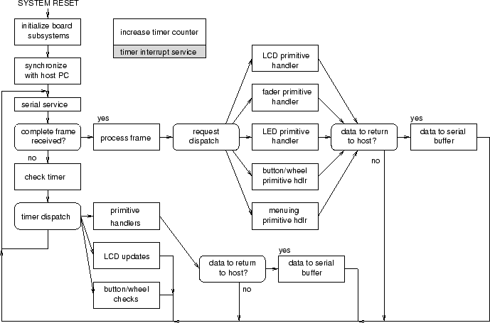
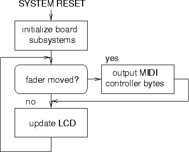
Next: Component Functional Design Up: Control Board Previous: Design Overview Contents Overall Functional DesignFigure 95 depicts a functional flow diagram for the intelligent mode of the control board firmware. At system reset, all components of the system are initialized. At that point, a host synchronization mode is entered, during which the host PC and the control board attempt to communicate and correctly exchange information. Upon successful completion of this synchronization, the control board sends configuration information to the host PC describing installed options, etc. At this time, the main program loop is entered. The serial devices are serviced, thereby processing incoming and outgoing data. Should a complete frame of incoming data be received, that frame is processed and interpreted. Assuming it contains valid command data, the command is dispatched to the appropriate user interface primitive handler. For example, if a command is received to generate a menu and return the chosen value to the host computer, the appropriate action is taken. In some cases, the primitive handlers immediately return data to the host computer, such as in the case of reading fader values, etc. In these cases, the data are immediately inserted into the serial buffer. After processing incoming frame data, or after no data have been received from the serial subsystem, the timer counter is checked. If this timer counter has reached particular cutoff values, functions are executed. Some user interface primitives require periodic servicing, such as the menu handling primitives. After the timer routines are serviced, or if no timer routines are to be serviced, control loops back to the top, and the serial devices are again serviced. This loop continues until the unit is powered off. Should, at any time, either the host PC or the control board become ``confused,'' the confused party shall re-enter synchronization mode. Both the firmware and the host PC software shall recognize, in normal operating mode, synchronization data coming from the opposite device. This shall cause that device to also enter synchronization mode, beginning the cycle again. The initial firmware developed for the board, and indeed, the only presently complete firmware, implements a ``dumb mode'' of operation. Figure 96 shows a functional flow diagram of this operating mode. Upon system reset, the various subsystems are initialized. At this point, the main loop is entered. In this loop, all of the faders are polled. If any of these faders have changed since the last poll, MIDI-like controller data are output on the serial port. This loop repeats until the system is powered off. This mode of operation is exceptionally limited, however, due to time constraints, the complete firmware system for the control board was not able to be implemented as designed. It is believed that the design is a good one, however.Next: Component Functional Design Up: Control Board Previous: Design Overview Contents Steve Richardson 2000-07-06 |
Table of Contents
| |
![[PDF]](/~prefect/images/pdficonsmall.gif) [Whole document in PDF 1.9MB]
[Whole document in PDF 1.9MB]