| |


Next: Audio Output Module
Up: Mixer Unit
Previous: Audio Mix Module
Contents
There is a single bus combiner board present in the prototype mixer
unit. Figure 86 shows the silkscreen/assembly layer
for this PC board. Table 7 shows the bill of
materials for the bus combiner board. Figures 87 and
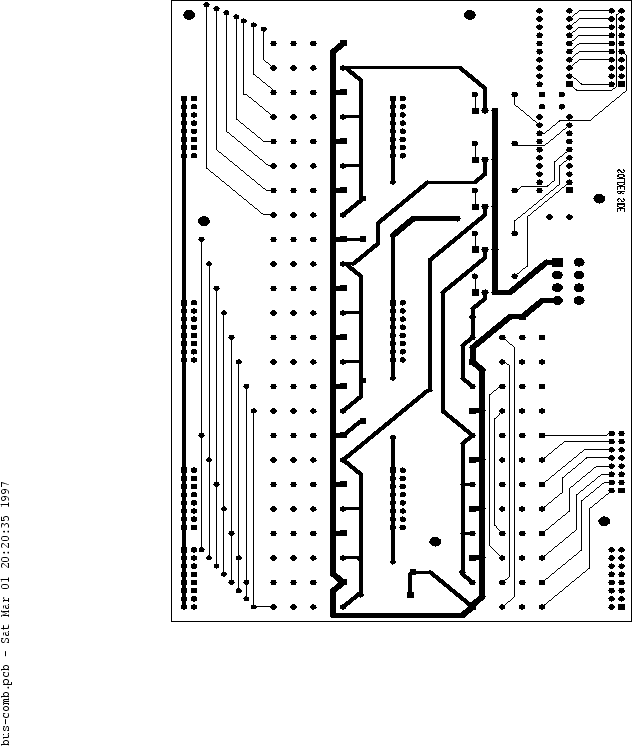
88 show the top and bottom routing layers.
Figure 86:
Audio bus switcher/combiner PCB, silkscreen/assembly drawing.
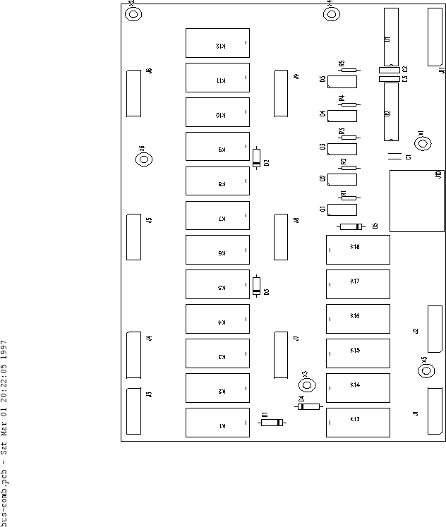 |
Table 7:
Bus combiner/switcher, bill of materials.
| REFDES |
QTY |
DESCRIPTION |
| R1 - R5 |
5 |
1K ohm 1/8W |
| C1 |
1 |
10uF electrolytic |
| C2,C3 |
2 |
0.1uF monolithic |
| K1 - K18 |
18 |
PED DPDT 5V coil relay |
| D1 - D5 |
5 |
1N4004 |
| Q1 - Q5 |
5 |
TIP120 |
| U1 |
1 |
GAL16V8 |
| U2 |
1 |
74LS373 |
| J1 - J9 |
9 |
16-pin DIP header |
| J10 |
1 |
Molex Mini-Fit Jr. 8-circuit right-angle |
| J11 |
1 |
20-pin DIP header |
|
Figure 87:
Audio bus switcher/combiner PCB, component-side routing.
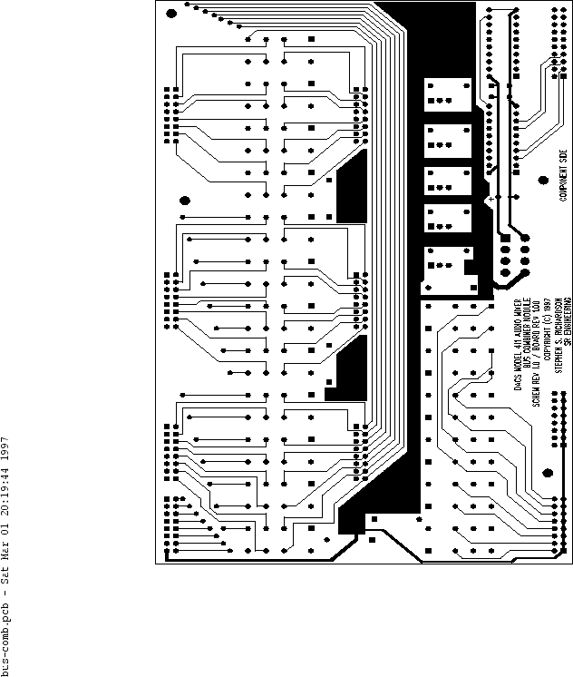 |
Figure 88:
Audio bus switcher/combiner PCB, solder-side routing.
 |
Next: Audio Output Module
Up: Mixer Unit
Previous: Audio Mix Module
Contents
Steve Richardson
2000-07-06
|
Table of Contents
![[PDF]](/~prefect/images/pdficonsmall.gif) [Whole document in PDF 1.9MB]
[Whole document in PDF 1.9MB]
[more photos and information]
|